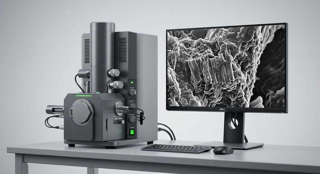
Key Capabilities
- High-resolution SEM imaging down to the nanoscale
- Microstructural and particle characterization
- EDS integration available for elemental mapping
- Suited to materials science, geology, and failure analysis
Models
Models in This Category
SEM — Scanning Electron Microscopy
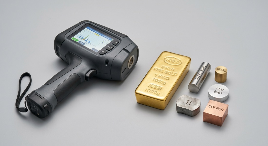
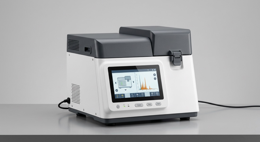
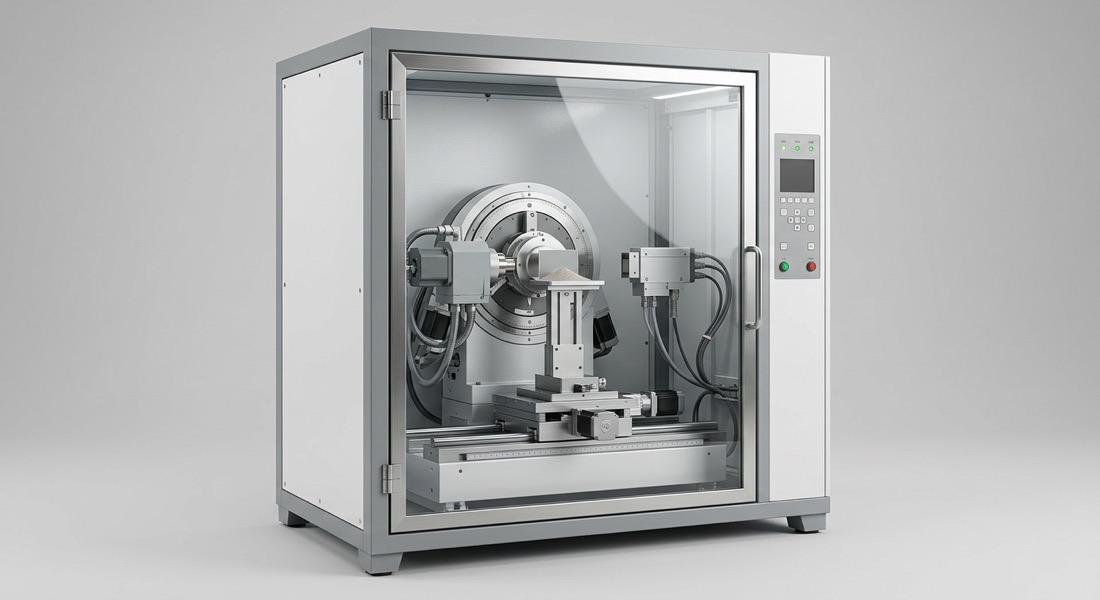
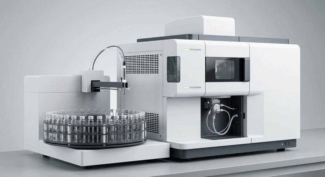
Ultra high resolution surface imaging and elemental microanalysis for materials science, geology, semiconductors and failure investigation.